The MEK600D2 has a standard configuration as supplied by Motorola. In this configuration it runs the JBUG monitor from a mask programmed ROM.
The memory map is as follows:

The memory space is not fully decoded though. The main decoder divides the 64k space into 8x 8k blocks. The JBUG ROM, for example is mirrored 7 times – which is probably how it is able to boot in the first place as reset causes execution to start at the top of memory.
The I/O appears even more curious with the address ranges of devices overlapping ie it would be possible to enable multiple devices at the same time using undocumented addresses. eg the One PIA is active when A2=1, the second PIA is active with A5=1, and the ACIA is active with A3=1.

The processor board has been modified with a 2k RAM board, so the RAM occupies the space from 0000H to 07FFH. Or at least that would be the case if other modifications had not been made.
It is also curious that there is a separate 128B RAM block set aside at A000H for the JBUG stack. This also, occupies a full 8k of memory space.
It seems that the MEK6800D2 expansion with external MOKEP boards was not entirely thought through by the time the D2 was released.
The first example is the 32kB expansion card which requires a contiguous 32k memory block which does not exist in the baseline design. The area from 2000H to 5FFFH was unused (the decode lines (2/3 and 4/5) go to the EXORciser interface.
The remaining area from 0000H to 7FFFH is reclaimed by disabling the expansion PROM at U12, and the re-allocating the RAM at 0000H to the area used for the dedicated JBUG RAM at A000H.
Helpfully, there is an application note that discusses possible modifications to accommodate various MOKEP cards. It highlights the VMA signal that can be externally activated to suppress onboard devices for particular addresses. It also introduces an Active signal which performs a similar function but is open collector so that it can be used by multiple devices. The Active signal was introduced by modification of the processor board:
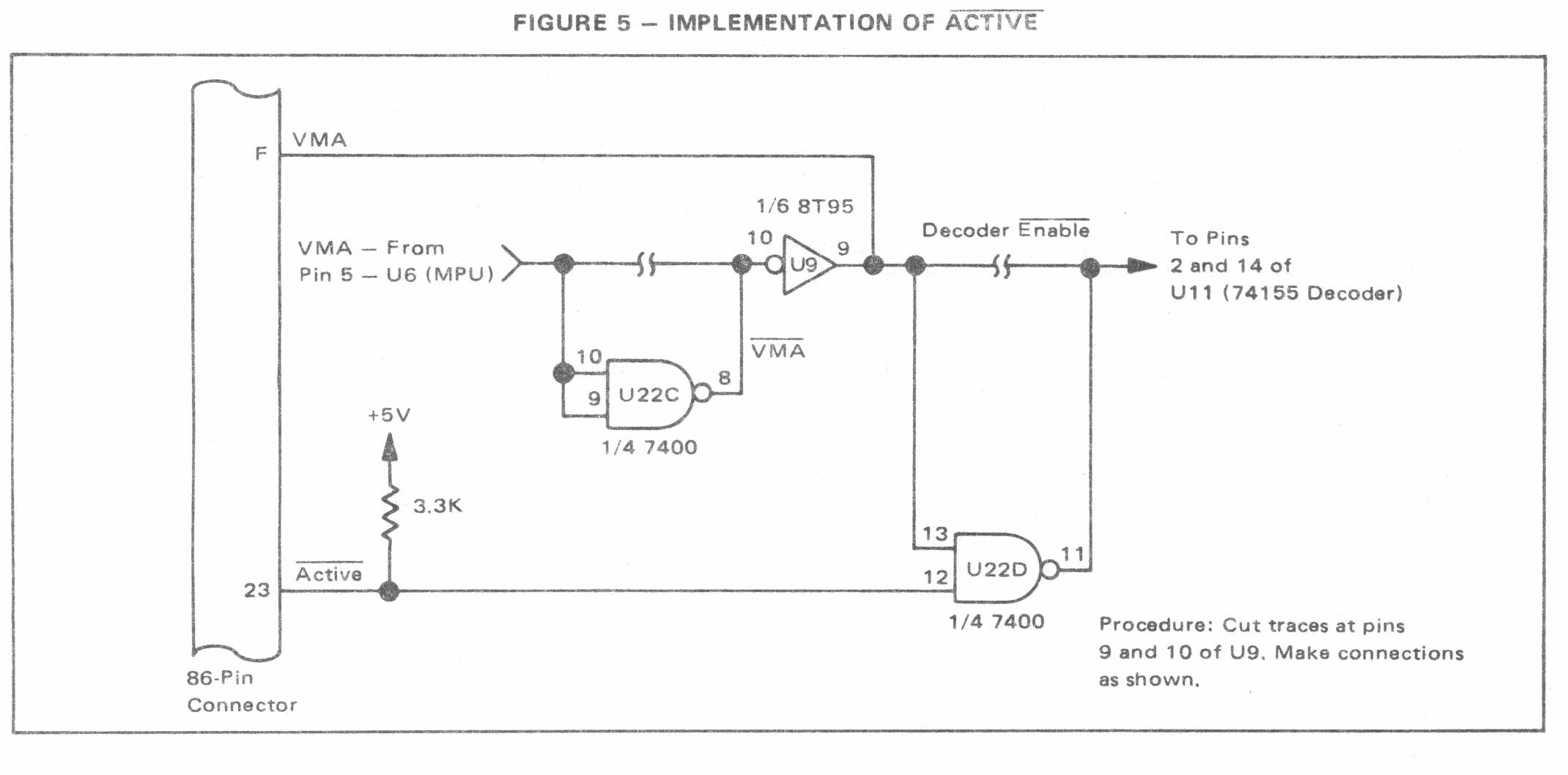
The Active signal is certainly used by the Video card and may be used by the RAM card. The Video card is active 8040H to 9FFFH so the Processor card decoder I/O output is active only for 8000H to 803FH.
The I/O Card can be configured for 4 different sets of addresses:

The card in this system is configured for option 2.
The I/O Card has not been loaded with the IEEE interface, but the decoding for it does seem to be present. On the face of it there is a potential contention with the Video card at 8058H.
Check what happens with I/O1 – the I/O card expects it but the processor card doesn’t provide it. There are some hints that the Video Card might provide it. What a curious thing.
The card has both the JBUG and CRT ROMs installed. The socket U10 has been modified so that both ROMs are enabled by PROM0_L at E000H. A switch is used to enable one ROM at a time.
There seems to be no device at C000H. It may be possible to move the ROM (U12) that was at 6000H to this location. This ROM has a lot of configuration options so it may be possible to configure the slot for a 2716 EPROM or even a 2732 EPROM. This would be very handy for routines to use the serial ports.
There are mods on the back of the keypad and display but they appear consistent with the schematic in the manual so perhaps they were covered by a note with the kit or were a service update. They are:
- Track cut at U20-2
- U20-2 wired to U11-6
- U11-4 wired to U17-7
- U11-11 wired to Ua8-1