The MEK600D2 has a standard configuration as supplied by Motorola. In this configuration it runs the JBUG monitor from a mask programmed ROM.
The default memory map is as follows:

The memory space is not fully decoded. The main decoder divides the 64k space into 8x 8k blocks. The JBUG ROM, for example is mirrored 7 times – which is probably how it is able to boot in the first place as reset causes execution to start at the top of memory.
The I/O appears even more curious with the address ranges of devices overlapping ie it would be possible to enable multiple devices at the same time using undocumented addresses. eg the One PIA is active when A2=1, the second PIA is active with A5=1, and the ACIA is active with A3=1.

The processor board has been modified with a 2k RAM board, so the RAM occupies the space from 0000h to 07FFh. Or at least that would be the case if other modifications had not been made.
The baseline board has a separate 128B RAM block set aside at A000h for the JBUG stack. This also, occupies a full 8k of memory space.
It seems that the MEK6800D2 expansion with external MOKEP boards was not entirely thought through by the time the D2 was released.
The first example is the 32kB expansion card which requires a contiguous 32k memory block which does not exist in the baseline design. The area from 2000h to 5FFFh was unused (the decode lines (2/3 and 4/5) go to the EXORciser interface.
The remaining area from 0000h to 7FFFh is reclaimed by disabling the expansion PROM at U12, and then re-allocating the RAM at 0000h to the area used for the dedicated JBUG stack RAM at A000h. It is not clear that the original stack RAM has been disabled. I will check.
The card has both the JBUG and CRT ROMs installed. The socket U10 has been modified so that both ROMs are enabled by PROM0_L at E000H. A switch is used to enable one ROM at a time.
There seems to be no device at C000h. It may be possible to move the ROM (U12) that was at 6000h to this location. This ROM has a lot of configuration options so it may be possible to configure the slot for a 2716 EPROM or even a 2732 EPROM. This would be very handy for routines to use the serial ports.
| Address Range | Device | Card |
| E400h-FFFFh | JBUG/CRTBUG (mirror) | MEK6800D2 |
| E000h-E400h | JBUG/CRTBUG | MEK6800D2 |
| C000h-DFFFh | Unused – use as ROM? | MEK6800D2 |
| A800h-BFFFh | 2kB Stack RAM (mirror) | MEK6800D2 |
| A000h-A7FFh | 2kB Stack RAM | MEK6800D2 |
| 8000h-9FFFh | I/O Space | MEK6800D2 MEK68R2 MEK68IO |
| 0000h-7FFFh | 32kB RAM | MEK68MM |
The I/O space presents some issues as it is shared by three cards.
Helpfully, there is an application note that discusses possible modifications to accommodate various MOKEP cards. It highlights that the VMA signal can be modified such that it will suppress MEK6800D2 devices under the control of a new backplane signal called ACT (active). This is also described in the MEK68R2 manual.
ACT can be generated by other cards to break into the MEK6800D2 memory space. eg an external card can assert ACT to push a device into the 8000h-9FFFh I/O space of the MEK6800D2.
ACT is open collector so that it can be used by multiple devices. The ACT signal was introduced by modification of the processor board:
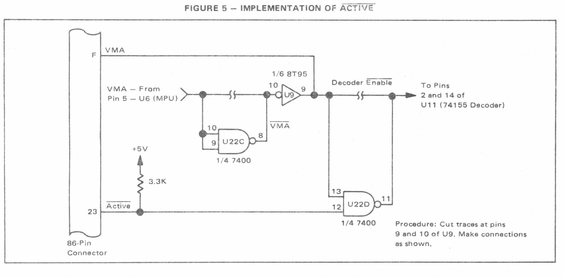
The effect of this signal is primarily to control the flow of data ie to ensure that the MEK6800D2 data transceivers allow data to flow from the backplane data bus to the card databus when an external device is read.
| Condition | Transceiver Direction | R/W_L | MEK6800D2 decoder output eg I/O_L |
| internal device is being read | out or off | 1 | 0 |
| internal device is being written | out or off | 0 | 0 |
| external device is being read | in | 1 | 1 |
| external device is being written | out | 0 | 1 |
This is really only problematic for the I/O space at 8000h to 9FFFh because this 8k space is shared with the MEK68IO I/O Card and the MEK68R2 CRT Card.
The ACT signal is certainly generated by the CRT card but does not seem to be generated by the I/O Card. To add to the intrigue, the I/O Card decoding relies on a signal, I/O1, which is, in this system, generated by the CRT Card. And there’s more; the ACT signal generation for the I/O Card appears to be handled by the CRT Card. Lordy, what a horses arse!
The CRT Card also generates I/O2 which is not currently used on this system but could be if another card (eg a bespoke I/O card) was added.
ACT should be asserted when:
- The I/O card devices are accessed
- The CRT card devices are accessed
- The CRT Card memory space is accessed
- The I/O2 range is accessed
If the I/O range 8000h to 9FFFh is selected then ACT is asserted except if the address is within the I/O1 range (8000h to 807F) and A6=0 ie 8000h to 803F. This is where the MEK6800D2 I/O devices are located. The I/O card must be configured so that the addresses are outside of this range.
The I/O Card can be configured for 4 different sets of addresses:

The card in this system is configured for option 2 but there is a further modification to A6 which removes an inversion. This adds 40h to each of the device addresses except the IEEE interface. This takes the devices into the range for which ACT is asserted.
The I/O Card has not been loaded with the IEEE interface. If it was then it would not work properly because its modified address would have A6=0.
The I/O space memory map looks like this:
| Address Range | Device | Card | ACT should be asserted. |
| 9000h-9FFFh | CRT RAM | MEK68R2 | T |
| 8044h-8047h | CRT Controller | MEK68R2 | T |
| 8042h-8043h | Peripheral Interface Controller | MEK68R2 | T |
| 8020h-8023h | PIA | MEK6800D2 | F |
| 805Ah-805Fh | ACIA | MEK68IO | T |
| 8058h-805Bh | ACIA | MEK68IO | T |
| 8054h-8057h | PIA | MEK68IO | T |
| 8050h-8053h | PIA | MEK68IO | T |
| 8008h-8009h | ACIA | MEK6800D2 | F |
| 8004h-8007h | PIA | MEK6800D2 | F |