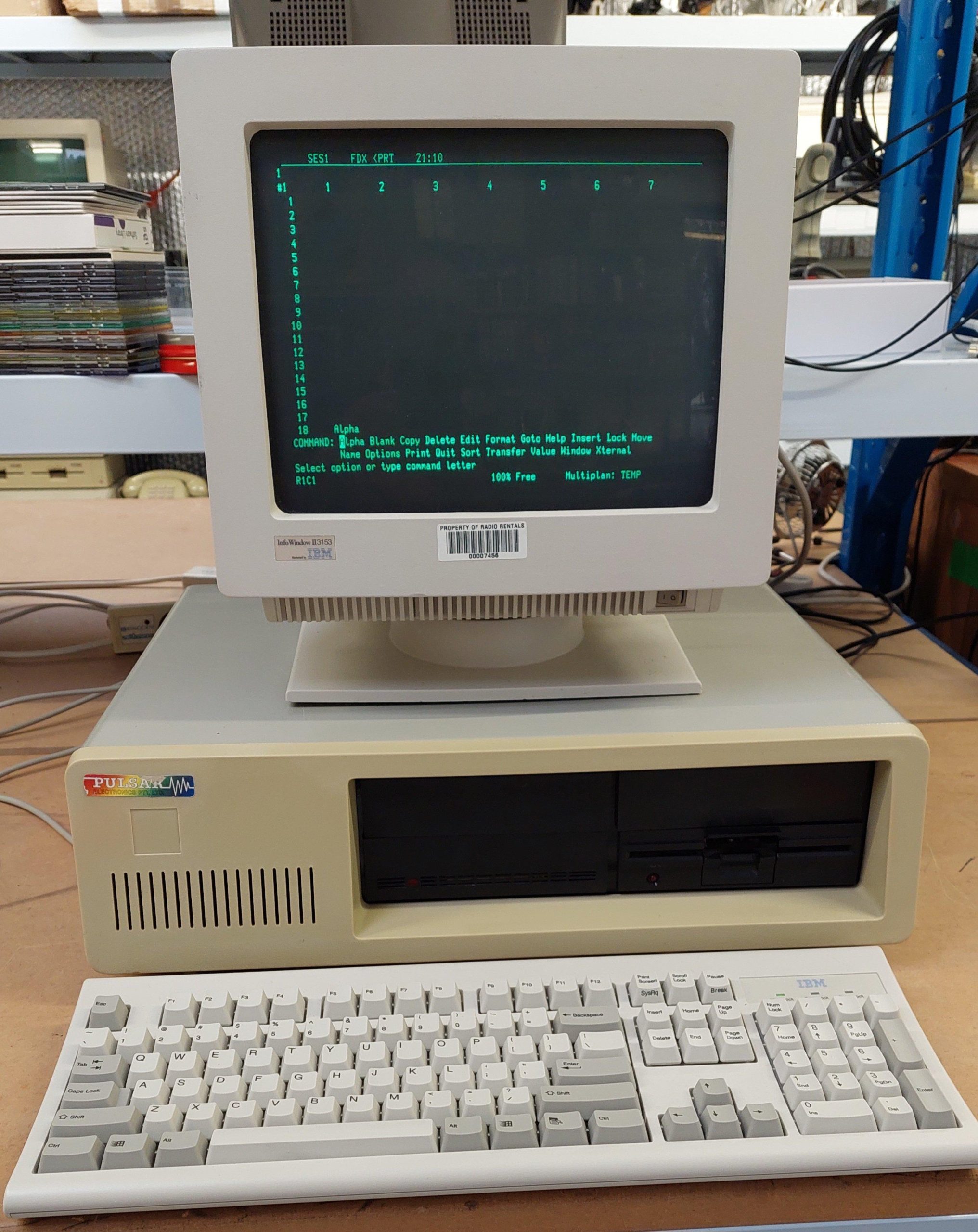
Inside the IBM PC style enclosure are 5 little big boards – one of which acts as a master to control drives and printers. The monitor is an IBM terminal, which is much younger than the computer.
The other four little big boards support 4 users via serial terminals. Each of these is connected back to the master via a serial line. These cards all run Turbodos. Each provides 64kB of memory for running CP/M programs.
The master provides access to a floppy disk drive and a SCSI hard disk – emulated with a SCSI2SD.
I connected it up to a serial terminal, but I couldn’t get anything out of any external serial port. The hard disk did not spin, so it may be a lost cause.
I had no boot disks for the floppy disk, although i thought it may be possible to create some from the 8″ disk collection. Many of the disks were related to Pulsar – both CP/M and TurboDOS.
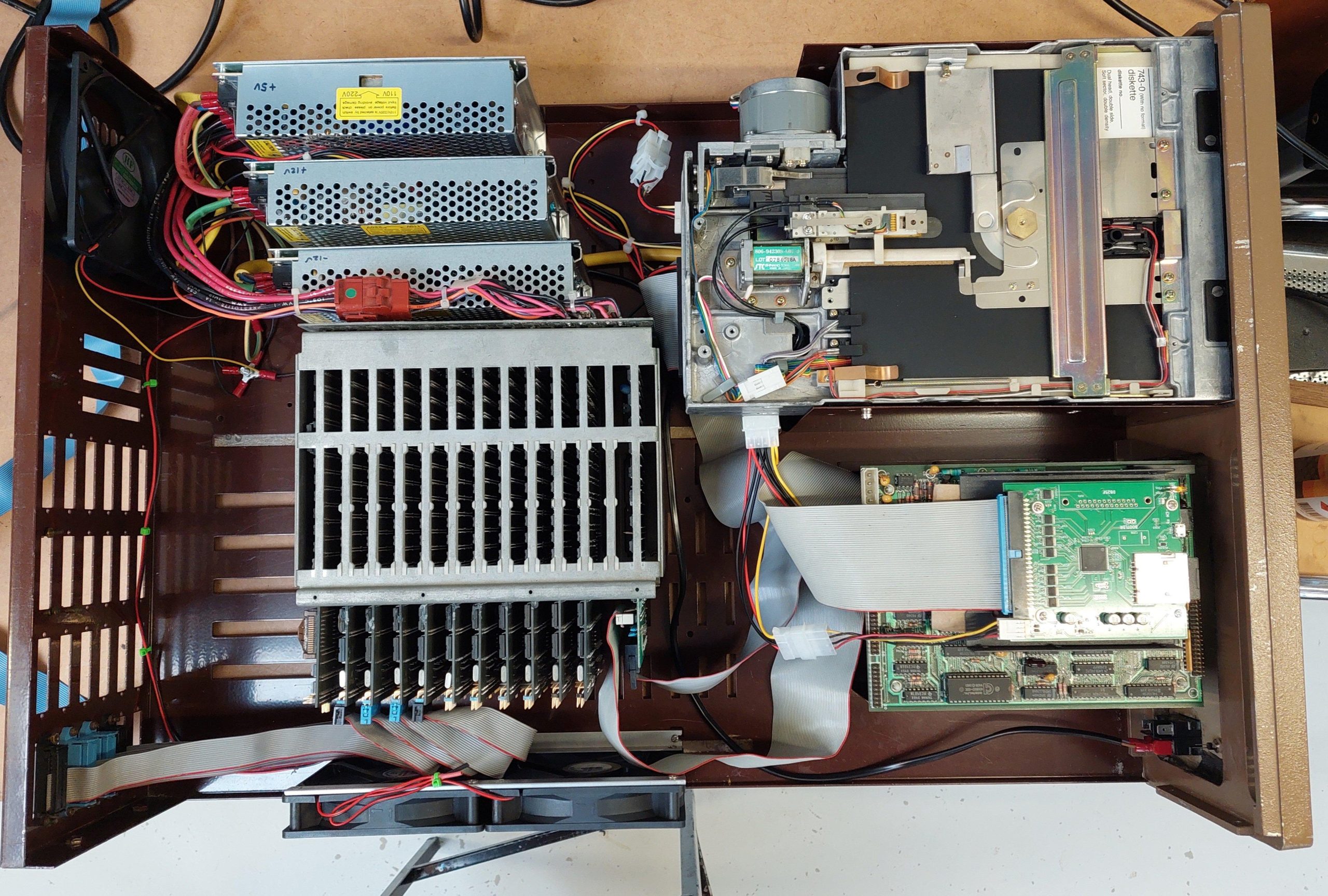
Working in the case was a little cumbersome, so I pulled the system right down to the boards:
It consists of:
1x Master LBB with STD and Floppy Drive Interfaces
4x Slave LBB (with a variety of options which are probably not used)
2x SASI/Dual Serial Boards
1x Mitsubishi M4854-342 High Density Floppy Disk Drive
1x NEC LR 56913Hard disk drive with Adaptec ACB-4000 SASI adapter
1x Sysquest removable disk drive with Adaptec ACB-4000 SCSI adapter (external to computer and mounted on it’s own baseplate)
There is a lot of variation amongst the slaves. Perhaps from card swaps over the years, or perhaps this machine was put together using whatever was in stock. Serial port connectors can be straight or right-angled, a bare header, or a shrouded header, sometimes with release levers.
Each of the slaves is connected via serial to the SASI/Serial cards. The master owns the bus and therefore the SASI/Serial cards. The slaves must not attempt to use the STD bus, so where the interface is loaded it has to be nobbled with track cuts.
There seems to be no reason why the slaves need to be in the unit – they could just as easily be located elsewhere but there is not a lot to be gained as either way a serial connection is required.
The serial ports on the master were used for printers.
I tested each of the boards with an MP7A Monitor ROM in a different chassis.
The master little big board does come up ok, so probably it was silent at switch on because that’s how the boot ROM rolls.
Two of the slaves were ok, but the other two were not working. One had a bad solder joint and the other had lost 12V connectivity because the track is very close to the board edge was severed. The damage would have occurred when I levered the board out of the backplane (there was no other way).
I could not get the master to boot from the floppy disk, even after adjusting the phase-locked loop as per Pulsar instructions. I parked that board and used a spare, which did boot.
From there the configuration tool was used to setup the slaves. There are a lot of questions about each slave. I took the easy options with automatic login of the privileged user.
The 7500 system uses a 5.25” drive rather than an 8″. As it turns out, the floppy disk drive in this unit, Mitsubishi 4854-342, is intended as an 8″ replacement – it even claims to be a 77 track drive although i suspect it’s good for 80.
The 50 pin host interface is connected to the 34 pin drive interface via a simple adapter. All up, this means that the 8” images can be written to HD 5.25” disks.
Looking at the simple 50/34 adapter board, I suspect that the drive has a couple of signals that may not be present on a 5.25” interface – Ready and 2Sides. I imagine that 2Sides is always asserted because there is no way for a 5.25″ drive to know if a disk is single sided. 8″ drives can.
The drive was cleaned and lubricated and tested ok with Imagedisk.
8” Pin
8” SIgnal
5.25” Pin
5.25” Adapter
Comments for Emulation with Gotek
2
TG43_L
Not used
4
6
8
10
2SIDES_L
2
REDWC_L
Not driven by controller or gotek. Pull down
12
14
SIDESEL
32
SIDESEL
16
18
HEADLOAD_L
4
Not Used
20
INDEX_L
8
INDEX_L
22
READY_L
34
DISKCHG_L
24
26
DS0
10
DS0
28
DS1
12
DS1
30
DS2
14
DS2
32
DS3
6
DS3
34
DIRC_L
18
DIRC_L
36
STEP_L
20
STEP_L
38
WDATA_L
22
WDATA_L
40
WGATE_L
24
WGATE_L
42
TRACK0_L
26
TRACK0_L
44
WRTPRT_L
28
WRTPRT_L
46
RDATA_L
30
RDATA_L
48
50
16
MOTORON
I wrote an HD floppy disk from 8″ disk image 8_257_02 (Pulsar Turbo V1.3 Master Configuration Sys 14 Config V24 Single User) using greaseweazle.
Pulsar was an Australian computing company located in Melbourne, Victoria. They made STD cards and computings systems based on the STD bus and often using TurboDOS.
TurboDOS is a multiuser/multiprocessor operating system that can execute CP/M programs.
Eight Z80 processors and two 80186 processors share an 8″ floppy drive and a SASI/SCSI hard disk, supporting 9 concurrent users. Each Z80 user gets their own 64k in which to run CP/M-80 programs, while the lucky 186 user scores 256kB in which to run CP/M-86 programs.
The master board, a 80186 board, loads the operating system from disk and, once it is up, it transfers the operating system to each of the slave cards.
All the rack-mounted cards are bona fide eighties cards. The rack and the 8″ drive are also of the time. The re-construction is new. I was able to find only very scant details of the Pulsar 9000, but i did have a complete set of cards and some software handbooks. It looked like a project!
Generously given to me by Michael from the ARC Group.
The Model I was originally released in 1977, but this one was made in about 1980. It has 16k of memory and has been highly modified.
It also came with an expansion unit with RS232 interface and 32k of additional memory. There was no disk drive, but that was only a minor obstacle.
It also came with an original monitor (probably not the ideal one to use with the expansion box), buffered cable to connect the computer to the expansion unit, a box which turned out to be a high resolution graphics mod, a joystick, and dust covers.
At its core this is a Cromemco 68000 system. It lacks the Cromemco chassis and Cromemco disk drives but it has a complete card set including:
a DPU Dual Processor Card with Z80 and 68000
a MCU Memory Control Unit
a 512MSU Memory Storage Unit connected to MCU via a MBus ribbon cable.
a 16FDC Floppy Drive Controller
2x TUART Twin UART
The chassis is an Australian made SME unit. I constructed the drive chassis based on an old STD chassis. It includes two Mitsubishi 8″ drives, a Mitsubishi 5.25 77 track drive and a gotek.
I have since added a modern IDE/CF Card for solid state storage and a modern 8MB RAM card.
It runs a very impressive unix-esque operating system called Cromix Plus. It supports up to 5 users via serial terminals. It can run 68000 programs and most programs written for CP/M. Each user can run multiple tasks.
I will probably do a lot of posts on this machine because it is fairly unusual and involved a lot of work. I do want to mention upfront that the solid state solution in this machine was made possible by the ever innovative John Monahan and software efforts of Damian Wildie.
The Cromemco Single Card Computer (SCC) design dates back to 1978 and this particular unit appears to have been made in 1978 or early 1979.
It has a Z80 processor running at 4MHz, 1kB of RAM, space for 8k of 2716 ROM, three parallel ports and one serial port.
The board was ROM-less but the binaries for the usual ROM set, MCB-216 were available online. These ROMs provide a monitor and 3k basic.
This means that with the addition of a terminal it’s possible to have a single card capable of executing programs that can exercise the S-100 bus.
I burnt the code into a couple of EPROMs, hooked up a terminal, and gave it a whirl. It fired up as if 45 years meant nothing. It starts up basic to start with but QUIT sends it to the monitor and B in the monitor sends it back to basic.
Programs can be saved to memory including to EPROM on particular Cromemco boards. They can also be saved to or read from the serial port.
The Monitor includes a memory test. I used it to check out a number of memory cards, with some success.
The Cromemco 64KZ appeared to be working fine. One board didn’t work because it expected pSTVAL to be driven and the SCC does not drive it. This was when i started to understand that the S-100 bus was not as “standard” as i had thought.
The main outcome was that i had a Cromemco memory card that was likely to be functional.
Cromemco CDOS is a lot like CP/M and can run CP/M programs.
There were sufficient cards to build a simple CDOS system. This is an interesting system in itself but is also a stepping stone to a Cromix system.
The cards are:
a DPU Dual Processor Card with Z80 and 68000
a 64KZ Dynamic Memory Card
a 16FDC Floppy Drive Controller
The DPU is overkill for CDOS but there is one very important CDOS program that is useful to the DPU: the 68000 memory test. That would prove to be handy later.
The 16FDC floppy disk controller has some handy bonus features: a serial port for a terminal and a monitor ROM running Cromemco RDOS.
A TUART can be added to provide parallel interfaces or additional serial interfaces for printers or other devices.
The RDOS Monitor version in the ROM is 2.01 which is capable of booting an operating system from a 5.25″ double density floppy disk – but not from an 8″ disk. The card itself has a 34 pin interface for 5.25″ drives and a 50 pin interface for 8″ floppy disk drives.
I connected a 40 track drive and created a disk from a CDOS image retrieved from the Cromemco GIT repository.
Continuing what had so far been a good run, the RDOS monitor came up after a few key taps (to autodetect the baud rate)and giving a b (boot) command initiated a successful CDOS boot.
I really should have stopped and had a good play with CDOS, because my lucky run came to a halt shortly after this.
Andrew, a friend from the ARC Group, has supplied me with a lot of funky gear including a box of S-100 cards, a couple of chassis, several 8″ floppy disk drives, and about 500 8″ floppy disks.
I never imagined that i would get an opportunity to work with S-100 bus. Components are difficult to find and, when they do appear, people expect an arm and a leg for them.
I had no idea if any of the cards were related to a particular system so all i could do was catalogue them and see if any patterns emerged. One pattern did emerge – there were several Cromemco cards including:
a Single Card Computer (SCC)
a 64KZ Dynamic Memory Card
a DPU Dual Processor Card with Z80 and 68000
a MCU Memory Control Unit
a 512MSU Memory Storage Unit connected to MCU via a MBus ribbon cable.
a 16FDC Floppy Drive Controller
a TUART Twin UART
Not knowing much about Cromemco, i started reading and a new world opened up. The Cromemco community seems to exist primarily as a Google Group with a huge repository on GIT. This proved critical because i did not have a skerrick of software or doco. There was nothing related on any of the 8″ disks that i had.
The repository includes a vast array of manuals, disk images, software etc.
I realised that there were sufficient cards to be able to build a system capable of running Cromix (a Unix look alike). It would consist of:
a DPU Dual Processor Card with Z80 and 68000
a MCU Memory Control Unit
a 512MSU Memory Storage Unit connected to MCU via a MBus ribbon cable.
a 16FDC Floppy Drive Controller
a TUART Twin UART (optional)
I’m not sure where these cards came from. Perhaps they had been used in a bespoke design or stripped out of a Cromemco system. If the latter, then the chassis and drives have not made it into my hands. I will need to use a third party chassis, drive enclosure, and drives. Also, notably missing from the list, is a hard disk controller such as the Cromemco WDI-II but i did see that it was possible to run a skeleton Cromix system from floppy disks. That would be good enough for me (until it wasn’t).
It was also possible to build a system capable of running Cromemco DOS (a CP/M look alike) and that seemed like a less intimidating option to start with. It would consist of the following:
a DPU Dual Processor Card with Z80 and 68000
a 64KZ Dynamic Memory Card or an MCU Memory Control Unit and a 512MSU Memory Storage Unit connected to MCU via a MBus ribbon cable.
a 16FDC Floppy Drive Controller
And there was an even simpler machine that could be built using just the SCC.
I started with the SCC and then used it to help locate faults in other boards. Then i moved onto the CDOS system which was also handy for finding faults in the 68000 system.
Having got a CDOS system to start up the next logical step would be to move on to a version of Cromix intended to work with the Z80 processor.
The Z80 Cromix requires at least 128kB of memory and because that is larger than the address space of a Z80 processor it needs to be managed. Cromemco uses a particular scheme to do that and, alas, i have only one 64k card (at least that’s what i thought at the time) that supports this scheme so i was blocked.
68000 Cromix has no such need. Instead, it takes advantage of the large address space of both the 68000 and the S-100 bus. The memory card combo of the Memory Control Unit (MCU) and the 512kB Memory Storage Unit (512MSU) is a compatible memory solution. All of this info was layed out fairly clearly in the 68000 Cromix administrator’s manual.
This is quite a sophisticated storage solution. Each 16 bit word is accompanied by 6 error correcting bits. The 512kB of storage is provided using 64 x 1 bit memory chips so the MSU has a total of 112 ICs. MCU can support up to 4 storage units. There is a memory bus that runs between the MCU and the MSUs.
ECC is off at power up and is optionally enabled by Cromix via a I/O port.
The initial system configuration consisted of:
a DPU Dual Processor Card with Z80 and 68000
a MCU Memory Control Unit
a 512MSU Memory Storage Unit connected to MCU via a MBus ribbon cable.
a 16FDC Floppy Drive Controller
On power on i was hoping that after a few keystrokes on the terminal that i would see the RDOS monitor prompt as i had seen with the CDOS arrangement. Nup. Nothing.
Adding the 64KZ back in, even with the MCU/512MSU present, allowed RDOS to function so the MCU/512MSU were apparently not responding at all.
I was able to use RDOS to quickly confirm that the MCU registers were working, although strangely they were located at 44H rather than the 4CH described in the manual.
I pulled all the cards except the MCU/512MSU and added the SCC back in. The SCC is self-contained so provides a stable work place for further testing. I could enter a simple program with the monitor.
A started with a simple write loop to a single location and then upgraded to a write-read loop.
After getting my bearings i could see that nothing was being written to the MSU. A lot of things have to happen for a memory write to work, and the SCC does not drive. SXTRQ_L and Z80/68k_L were both negated with pullup resistors.
Also, obviously, the SCC doesn’t drive the A[23:16]. The MCU pulls these high so when using the SCC the address selection switches must be set for FF rather than 00.
The MCU does have quite a job to do – it must arbitrate at least three different requests:
Read
Write
Refresh
There’s also 8 and 16 bit transactions. And the error detection and correction must also have quite an impact.
As part of dealing with each cycle, it must control the data paths and the DRAM signals eg CAS, RAS, and Write. IC24 initiates the cycles; CYCLE START indicates the start. CT[2..0] indicate (I think) the type of cycle.
IC45 steps through the sequence of events and times the length of each step. IC30 is a lookup table that determines (amongst other things) the duration of each step based on the step number and the cycle type.
IC46 is a large lookup table that generates a bunch of signals based on the step number and the cycle type.
The activity was complicated because the SCC generates external reads and writes even when accessing internal RAM and the presence of the refreshes. I tried masking the MemR signal and disabling the refreshes but these both had the side-effect of locking up what is, in effect, a very complicated state machine.
In the end it wasn’t necessary, and it was possible to see the write cycle on the scope. The output signals made no sense so either the lookup table was toast or there was a bad connection. Sure enough closer inspection revealed a that the pins on IC46 had developed a brown coating (it’s socketed). I should have checked this on day one, but i wouldn’t have learnt nearly as much!
The reset is interesting – a lot of the MCU is reset by the POC signal – probably so that the RAM is refreshed through a reset.
I cleaned all legs on all socketed ICs and suddenly there was action. I did find that once the MCU/MSU became responsive there were some issues with the Z80 monitor on the SCC – specifically when quitting BASIC to enter the monitor was unsuccessful. If the board is disabled (eg set a DIP switch on the MSU to off, then the monitor starts fine. Once started the DIP switch can be returned to one apparently with no ill effect.
Alas, there are several RAM errors and all the chips are soldered in. Worse still the 4 x 64kx16bit banks appear to be interleaved. That means that all of 64 RAM chips need to be working just for the bottom 64k to be available. And that’s ignoring the error detection and correction etc. Ouch. On the bright side it’s possible to partially test each RAM chip from the SCC.
I did different fills at different addresses to detect address line issues.
There were a lot of address errors where bits were written to the wrong address, eg because an address line was stuck in an IC. That yielded another 12 duds.
Most of this i could do from the SCC Monitor.
The pattern of ICs on the 512MSU is like this:
I think that the MCU/MSU always performs 16 bit transactions even when an eight bit transaction is requested. And I think it does this by using read-modify-write cycles ie it writes back the contents of the unchanged byte as well as calculating the new error detection and correction bits. Tricky!
I made numerous attempts to install 68000 cromix from the source images, but i encountered numerous problems (will cover in another post). I eventually concluded that i must have a residual hardware issue and was able to confirm this via CDOS – in particular, i could copy files reliably when i used my 64KZ but not when i used the MCU/MSU.
The MCU/MSU RAM checked out well with the 68k RAM test but i thought i’d try the 8 bit test as well and that showed an issue with the delay test. I was not able to reproduce the issue by manually changing RAM values in the monitor, so it must be quite a specific situation that triggers it. The delay test is really made for the 16KZ, so the chip identifiers were meaningless – the memory organisation in the MSU is completely different to that of the 16KZ. Nevertheless, it did indicate that the fault was in bit 8.
I figured there were 8 x “bit 8” chips on the MSU and i had already replaced 2 so i replaced the other 6. Having done that, it passed the delay test and eliminated the erratic behaviour. Consequently, my personal well-being improved dramatically.
I used a socket with each replaced RAM chip, so they are visible in the photo. A total of 24 chips out of 64 memory ICs. I think there’s a fair chance that others will develop faults over time.
I have never checked the ECC ICs, but i would expect that about 1/3 of the 24 ICs will be faulty.
I don’t know why the failure rate has been so high. Sure, 4164 RAMs do fail, but i have not seen this sort of rate before. These are TI TMS4164-15NL with date code P8231.