I had been quite intrigued by the idea that the Cromemco Z80 Monitor and 3k Basic could save programs to EPROMs instead of, for example, paper tape, magnetic tape, or floppy disk.
I was thinking particularly of my Cromemco Single Card Computer (SCC) but the same trick is possible using a Cromemco ZPU Card.
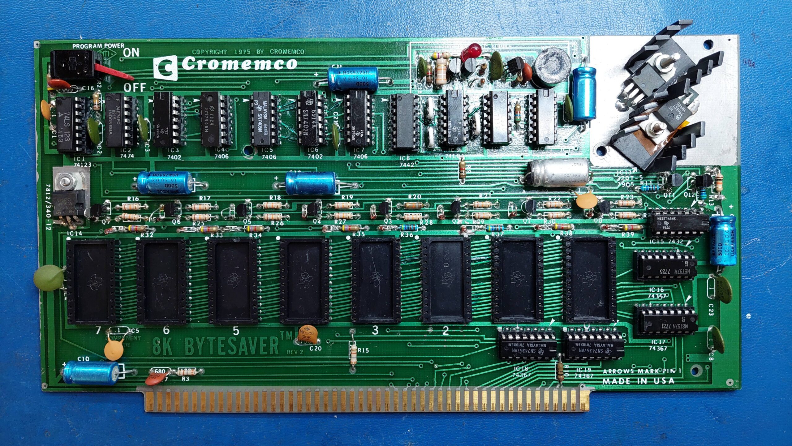
To do this requires a card capable of programming an EPROM eg Cromemco 8k Bytesaver, 8k Bytesaver II, or a 32k Bytesaver.
The cards that i had seen on ebay were in the States and were prohibitively expensive, even before adding the postage. Fortunately, though, an 8k Bytesaver come up for sale in Adelaide. Despite its poor condition and significant price, i acquired the card so that the itch could be scratched.
The 8k Bytesaver was a milestone card; the first S-100 card to provide EPROM storage. Prior to this, machines were typically bootstrapped by entering a boot-loader at the front panel. This card was released in 1976 shortly after Intel released the device that made it possible, the 1k x 8 bit 2708 EPROM.
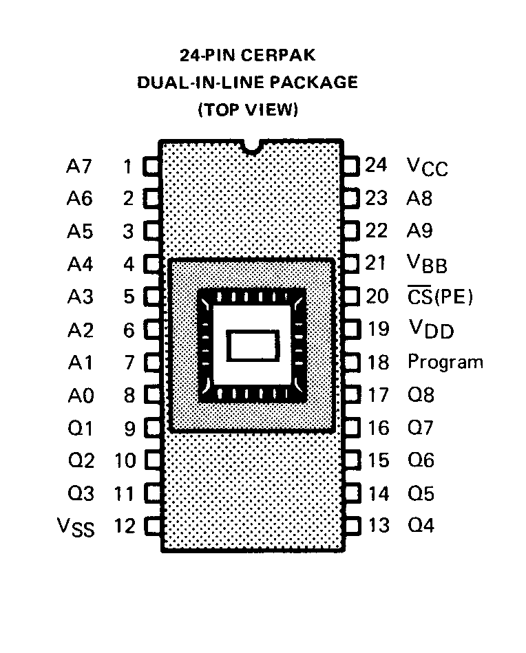
The 2708 is not as easy to work with as later EPROMs. Even for reading it requires +5V, +12V, and -5V supplies. For programming, it requires CS to be taken to 12V and an additional programming voltage at 26V.
The EPROMs themselves are not particularly common, but i have a bunch that i have previously imaged, and they can also be purchased for about AU$6 each.
I wasn’t sure that the 8k Bytesaver would work with the SCC (the SCC manual was a little ambiguous), but i also had the option of using a ZPU.
The purchased card had been modified to use 2732 EPROMs with, as far as i could see, no ability to program the EPROMS. Many tracks had been cut and components removed. Even the original heatsink had been replaced with a lesser version.
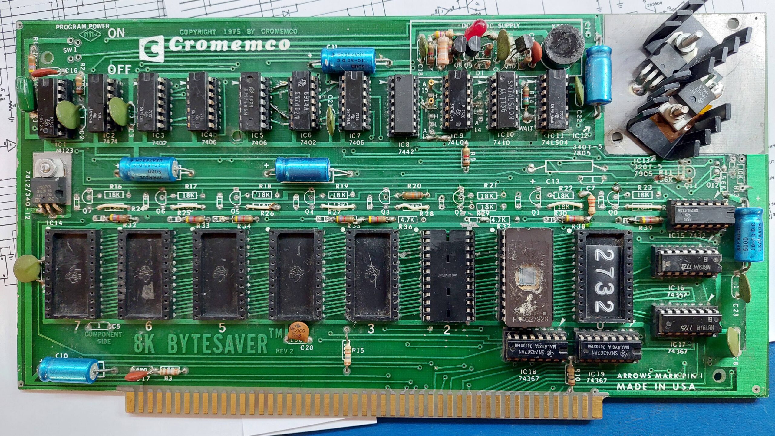
As a 2732 EPROM card it was useful, but it was nothing i couldn’t put together on a prototype card as i had done once before. Fully restored it would be far more interesting so that’s what i decided to do.
Cromemco sold the card as a kit, it looks like it was assembled by an amateur, it had been modified (probably twice) by an amateur, and was now about to be restored by an amateur. Some cards are born to a life of hardship.
I checked the programming power supply first; a terminal fault would mean there was no point proceeding. It worked fine.
The programming switch had been stolen, so i stole one from a faulty Lexitron floppy disk controller board. Not sure what to do about the heatsink.
One socket had been replaced with a different type. I found a donor board with the matching type and swapped it out.
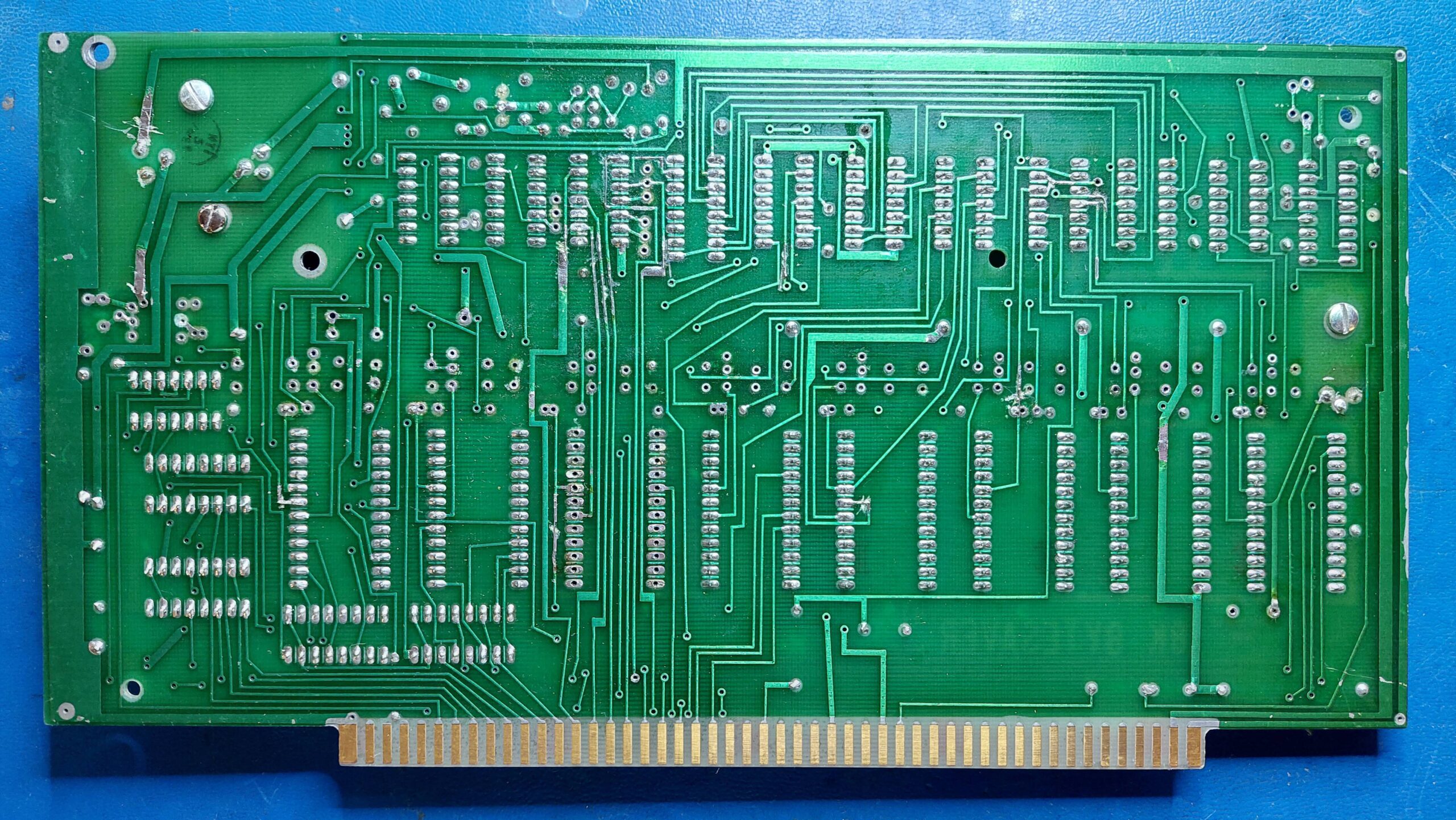
I started by removing everything that wasn’t supposed to be there and tidied up the original soldering.
Then i started looking for the track cuts. There were a lot of them on both sides of the board. Many cuts had been made and then repaired. They were a bit rough with deep gouges to the fibreglass and large gaps in the copper.
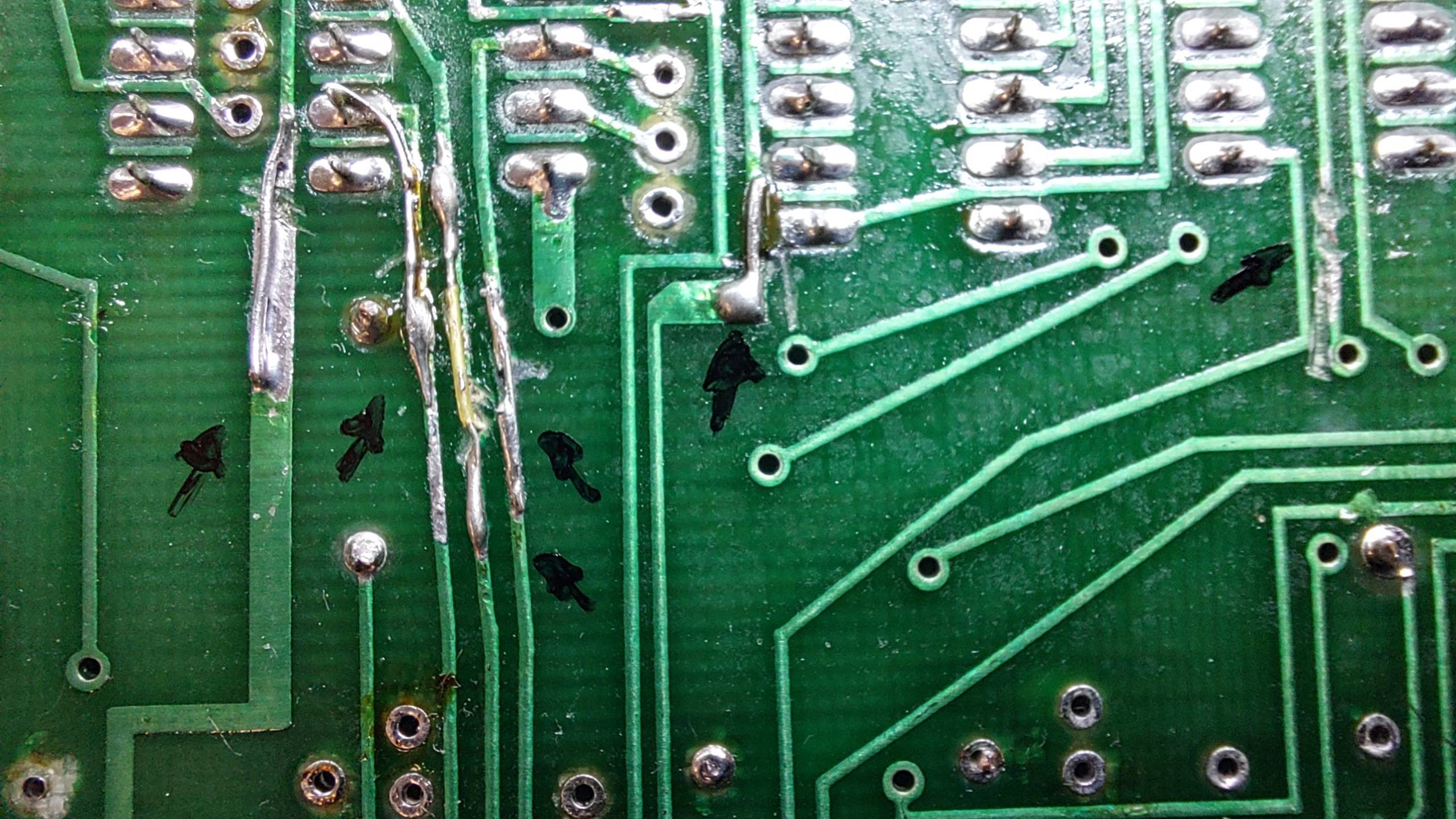
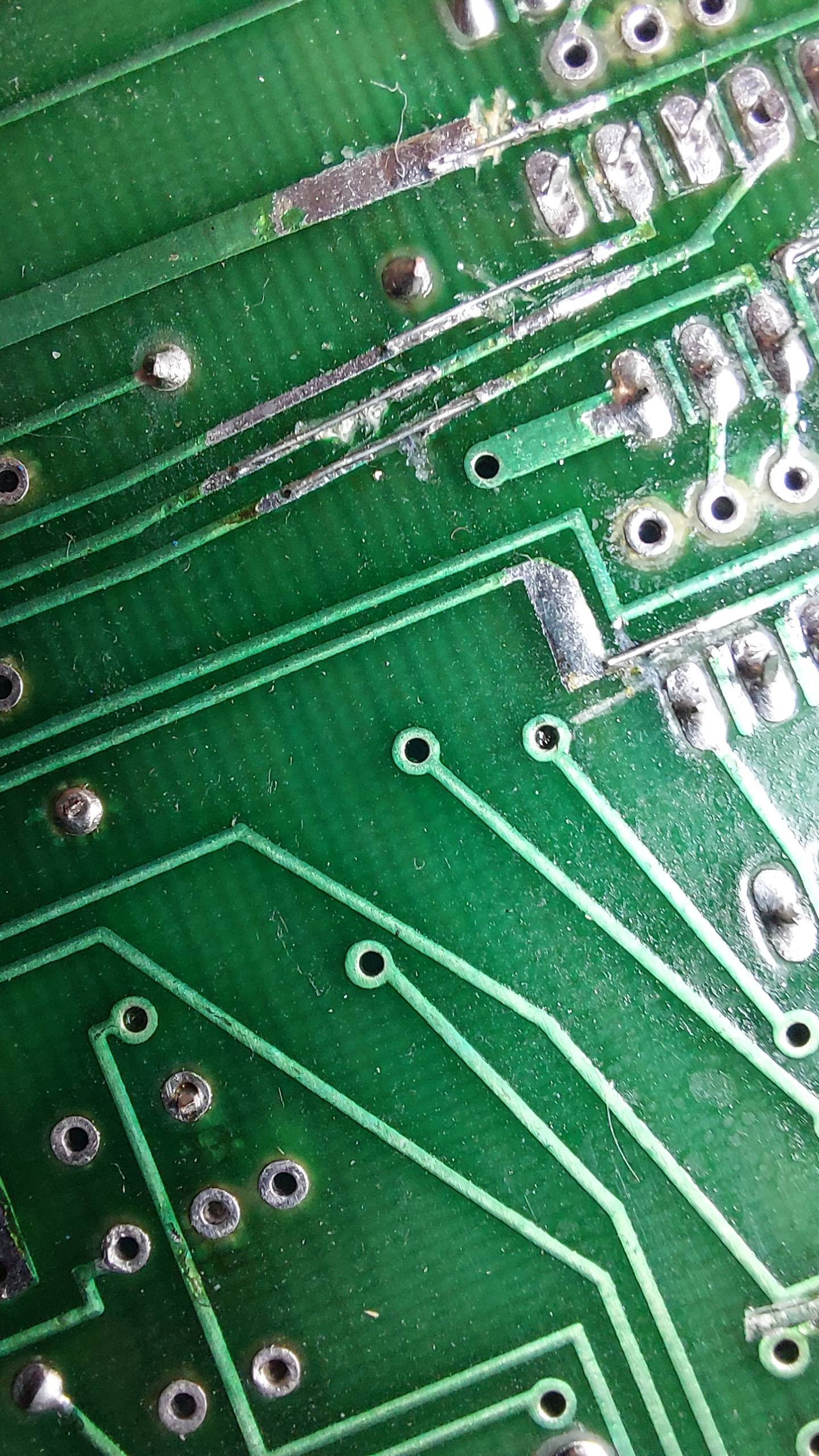
Each was made good as neatly as possible with the available skill.
I covered the mods with UV cured solder resist just for appearances. It can’t be perfect, but it is a lot better.
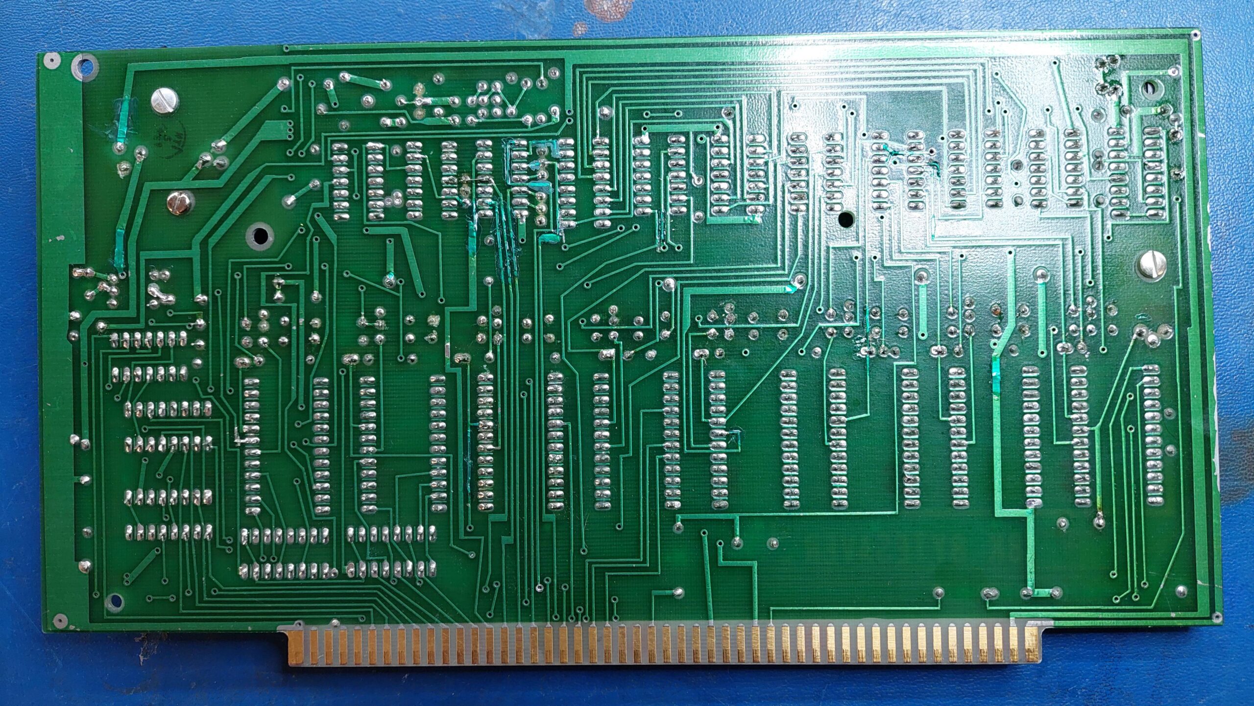
I replaced all the missing components, which were fairly generic.
I gave the board a good wash and all the sockets and ICs were given a couple of rounds of deoxit. Many of the ICs had very black legs – i suspect that many of them had silver-plated legs.
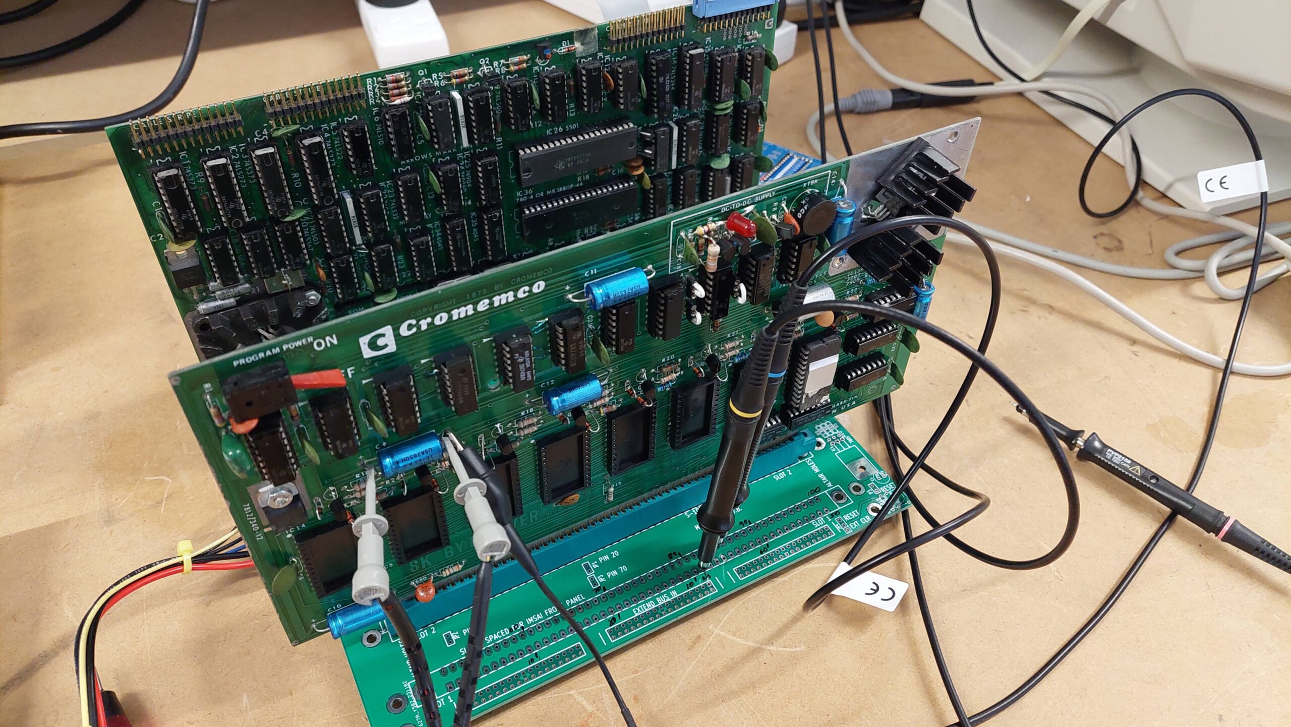
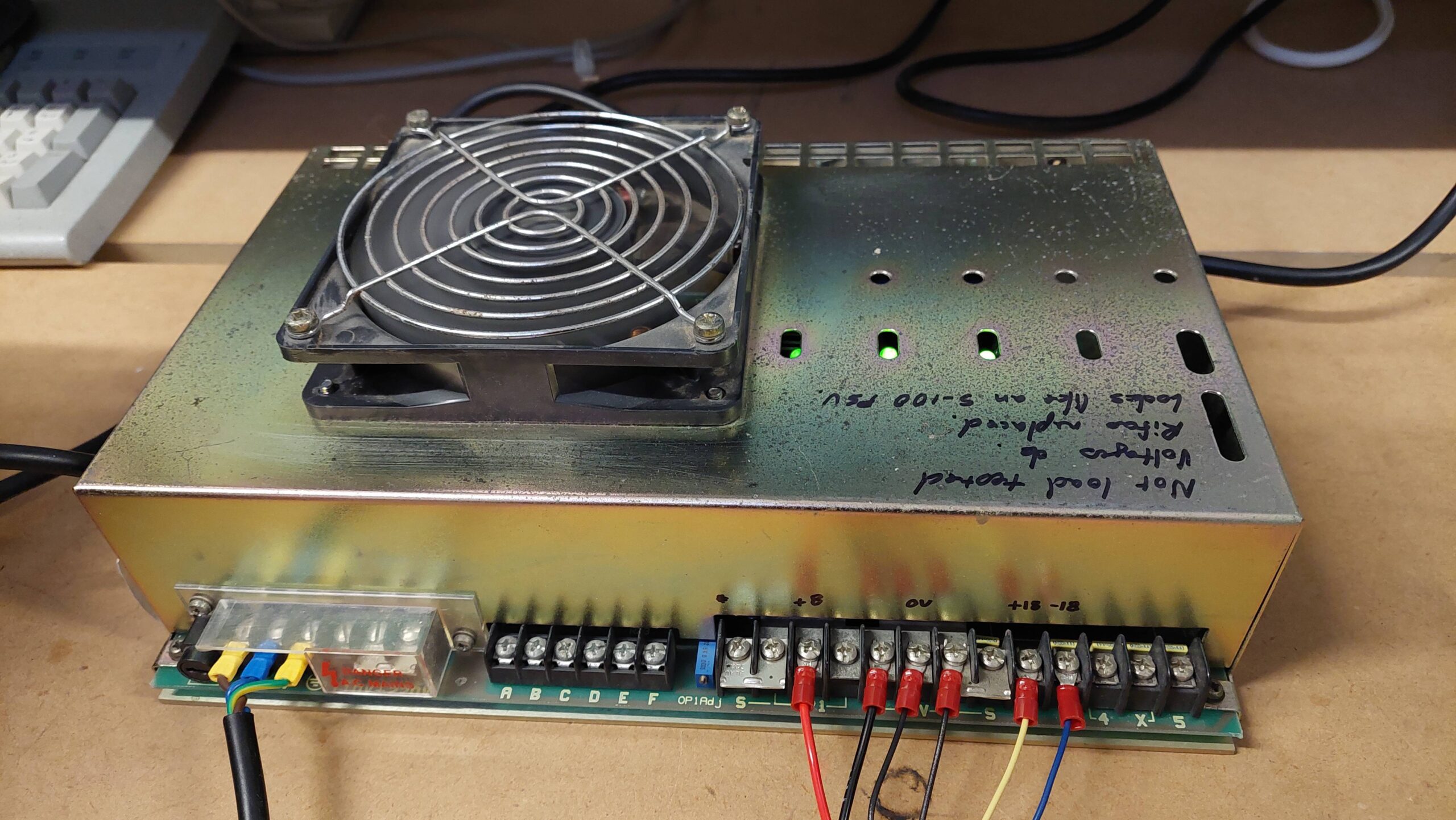
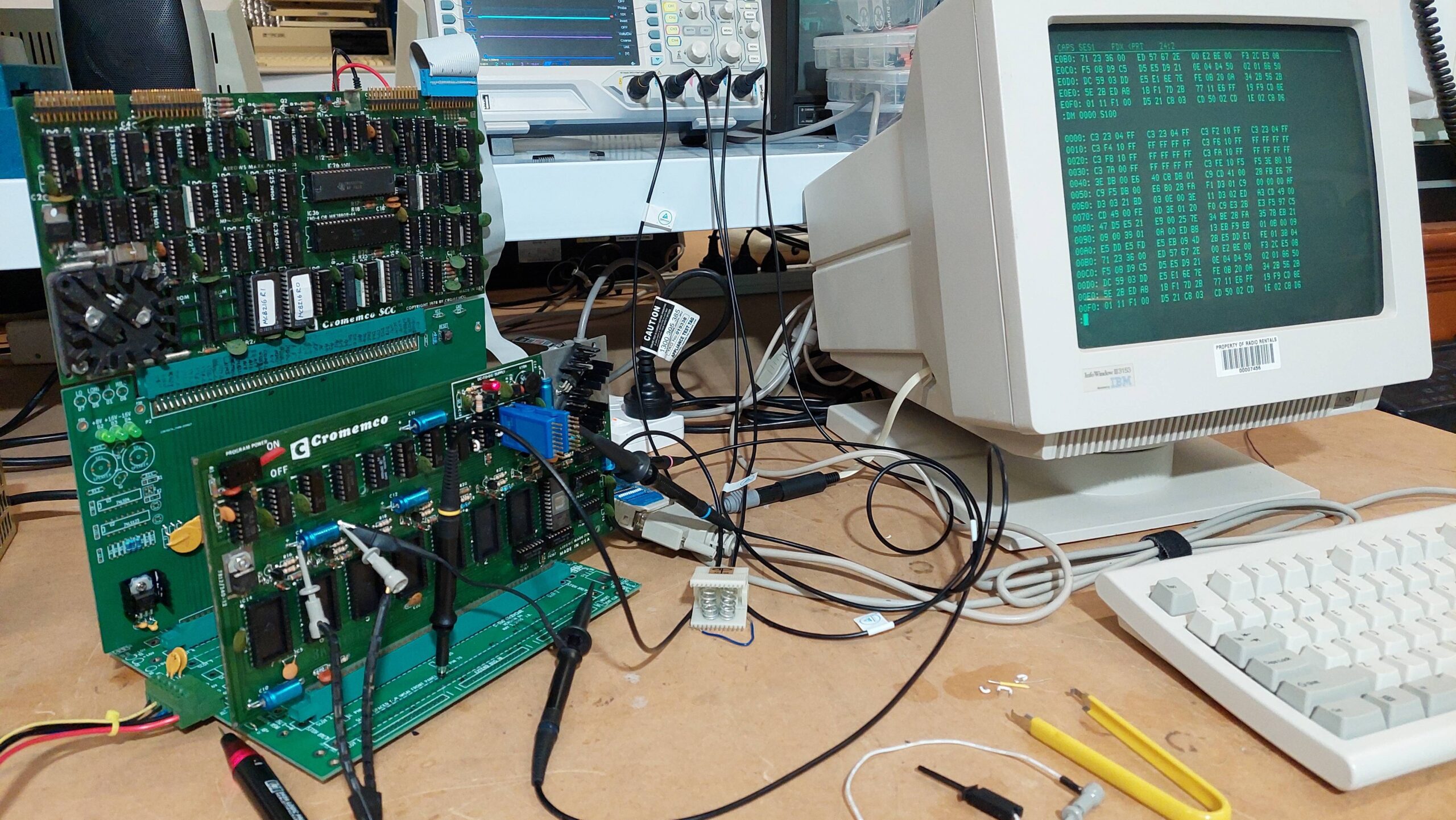
With my only two racks in use, i needed to get around to building up a third backplane. This one is based on the S100 Computers 9 slot backplane. Being lazy, i added just the two connectors that i needed.
I was fortunate to have picked up a monster of an S-100 power supply off FB marketplace a while ago. With the power loom made, it was ready to go.
I checked the supplies without any ICs inserted. All good. Then i added the ICs.
The simplest test option for me was the Cromemco SCC. It had been a while, so i had to re-acquaint myself with its operation. It has 2 x 2kB EPROMs holding 3k Basic and the Z80 monitor. The SCC talks with a user via a serial monitor.
On power up, the user has to send a couple of carriage returns so that it can detect the baud rate.
I configured the Bytesaver to be at E000H which is well away from the SCC EPROM/RAM space. It uses no I/O space. Attempts to write to the card are treated as programming cycles with lengthy wait states inserted.
There are several manual scans available, and they do contain schematics, but the resolution is such that they are very difficult to read. This is not helped by Cromemco’s policy of prioritising low sheet count over clarity!
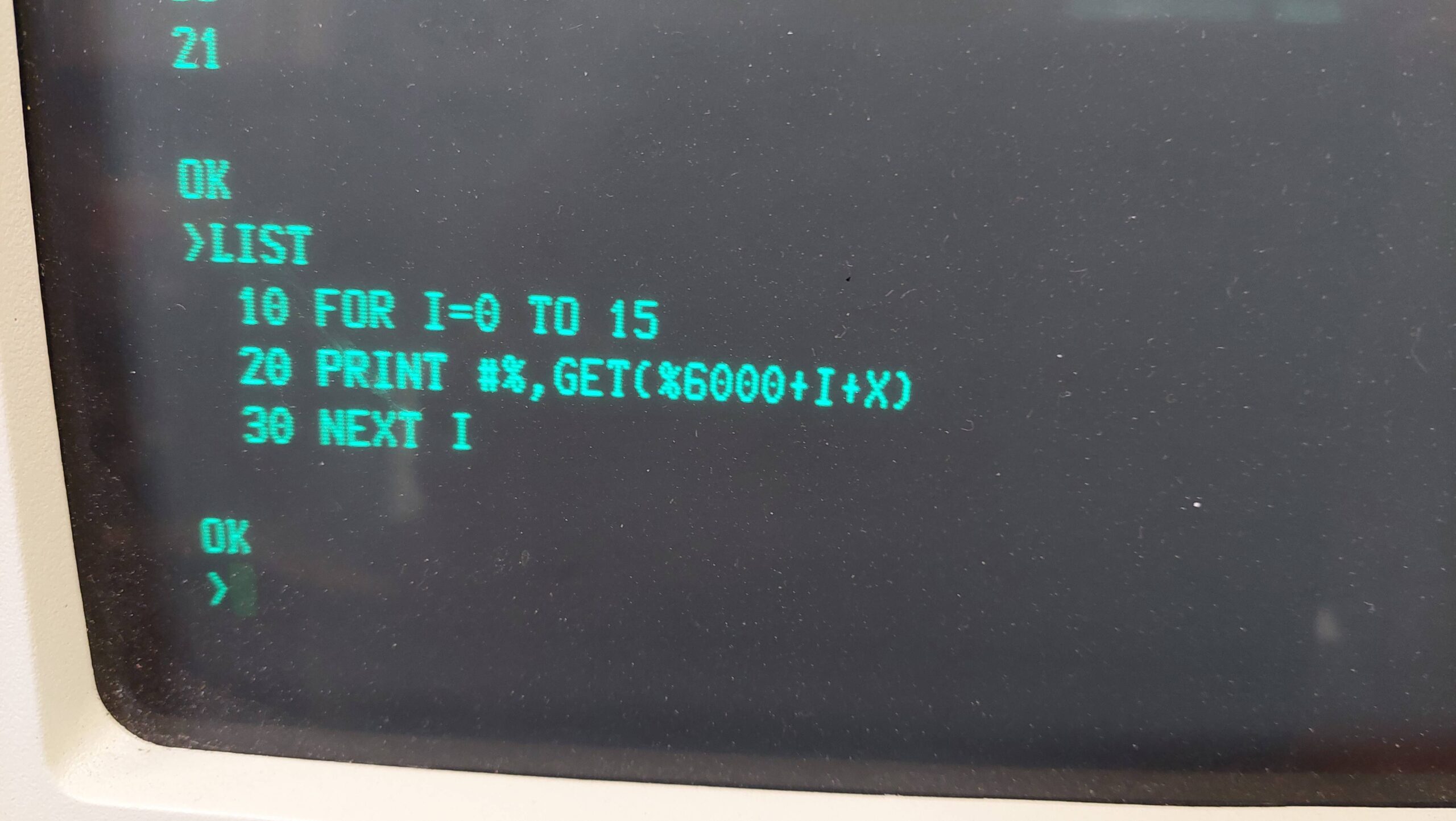
I was not able to reliably quit from the 3k Basic to the Z80 monitor so i did a lot of the debugging in Basic (pic with base address at 6000 rather than E000).
I checked a few signals without EPROMs, and then tried reading some EPROMs that had previously been imaged. I found the fifth EPROM overlapped with the first (a bad address line from the SCC) but once that was corrected (IC48 74LS244) it all looked good.
Then i removed the EPROMs and had a look at the programming cycle. This cycle relies on monostables to do the timing and they weren’t. I replaced the IC1 74LS123 and got some cycles that looked good.
Write cycle with switch OFF:
MWRT, Board_Select, EPROM CS (pin 20), EPROM Program (pin 18)
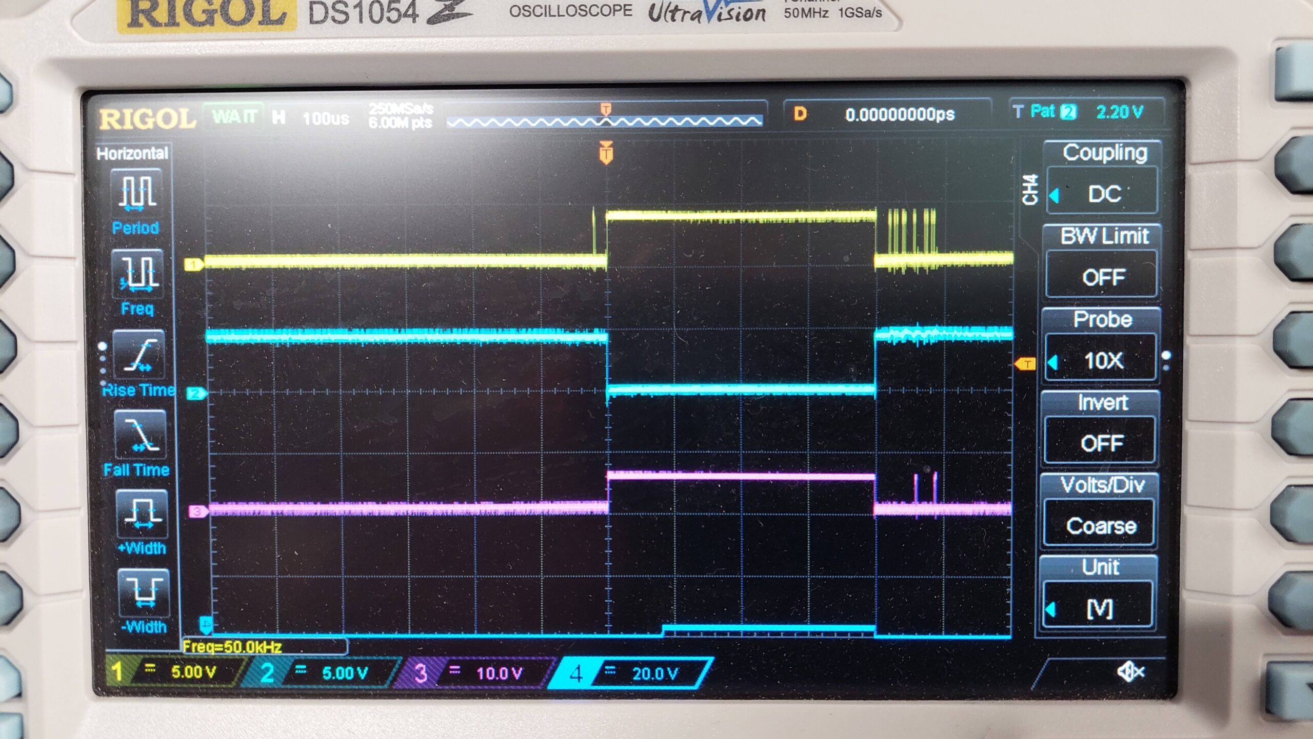
Write Cycle with switch ON:
This is how it should work according to the manual. With the programming switch on the CS pin rises to 12V and then a short time later the programming voltage is applied.
I looked further at the issue with the transition to the Z80 monitor. I found that it is fine if the PRDY signal is disconnected during the transistion, eg remove IC16-3 and connect with lead after transitioning. This is not a long term solution!
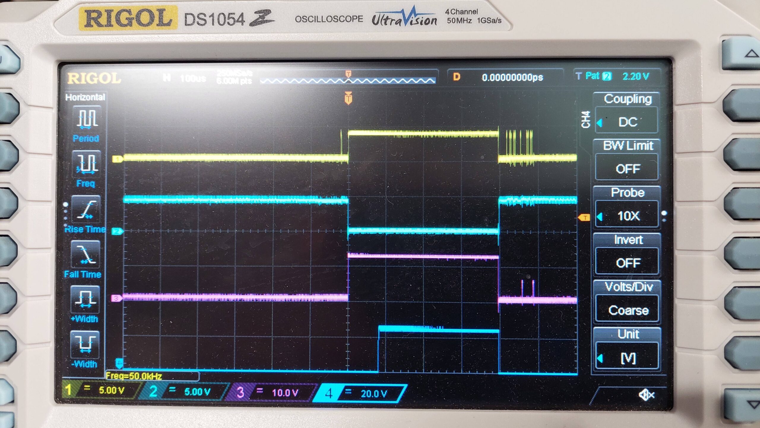
This is what it looks like when QUIT works:
WRT, Board_Select, EPROM CS (pin 20), PRDY
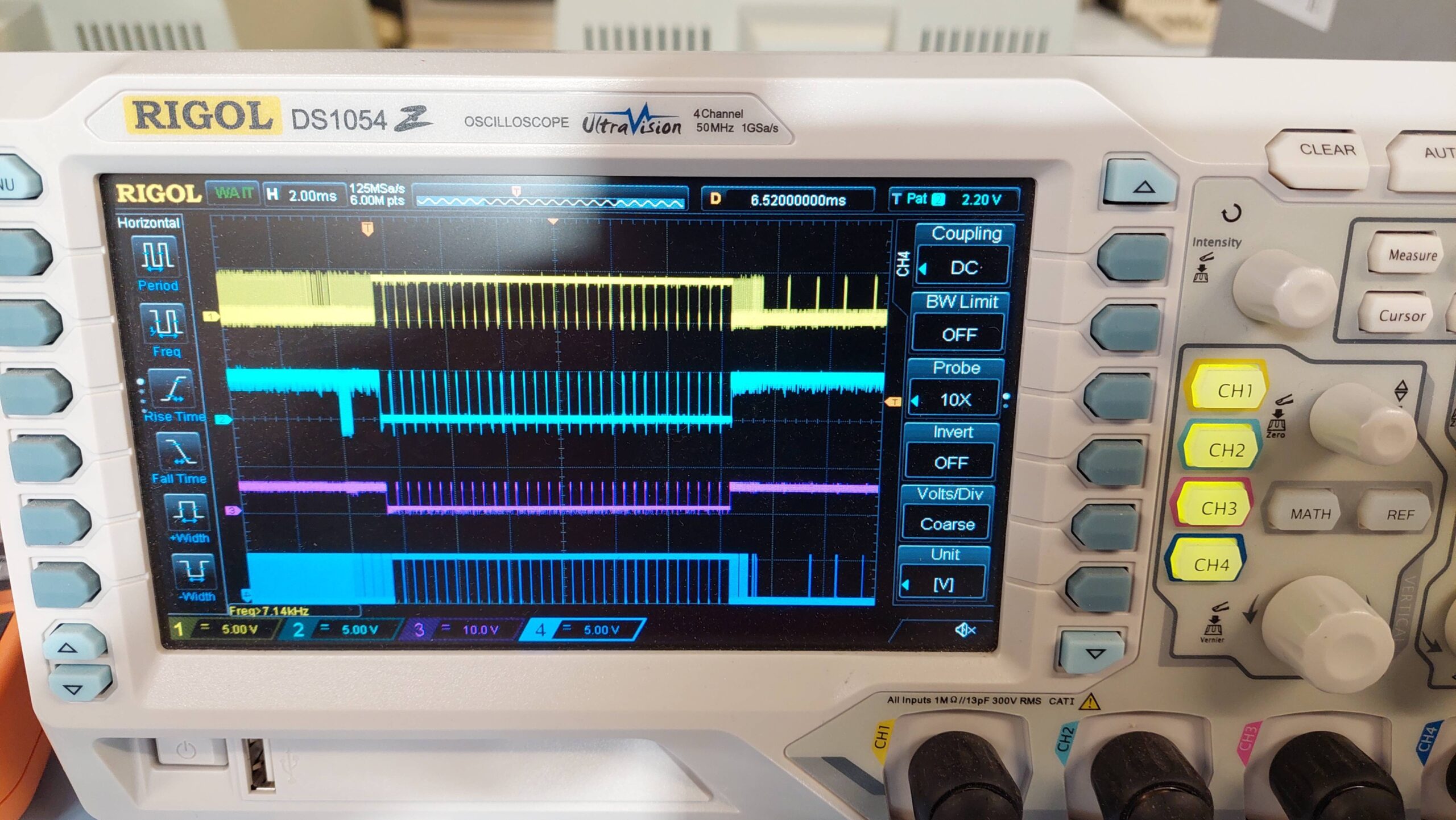
It seems to do 32 writes – is it scanning for available RAM with a write/read check?
I tried replacing the 74367 that drives PRDY. This seemed to have an effect. The transition would work repeatedly. And then it didn’t work repeatedly. And so on and so forth.
I then replaced all the 74367s without any very good reason. It will take some time to work out whether the issue has been resolved.
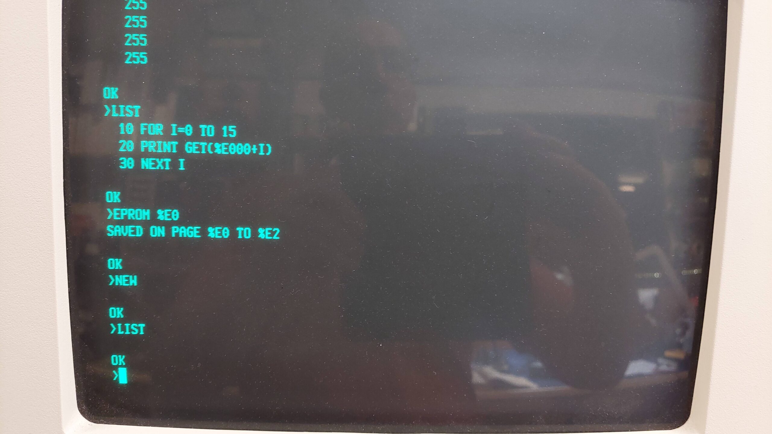
I tried programming an erased 2708. Remarkably, it programmed just fine! I used the Z80 monitor to copy the first 1k of the SCC ROMs to the blank 2708:
P 0000 S400 E000
I think it verifies during programming, but i verified it anyway:
V 0000 S400 E000
I eyeballed some of the data because i didn’t quite believe it.
It takes about 6 minutes to program a 2708, so a large program would take some patience.
After erasing the EPROM, i tried saving a program in 3k Basic. Victory!
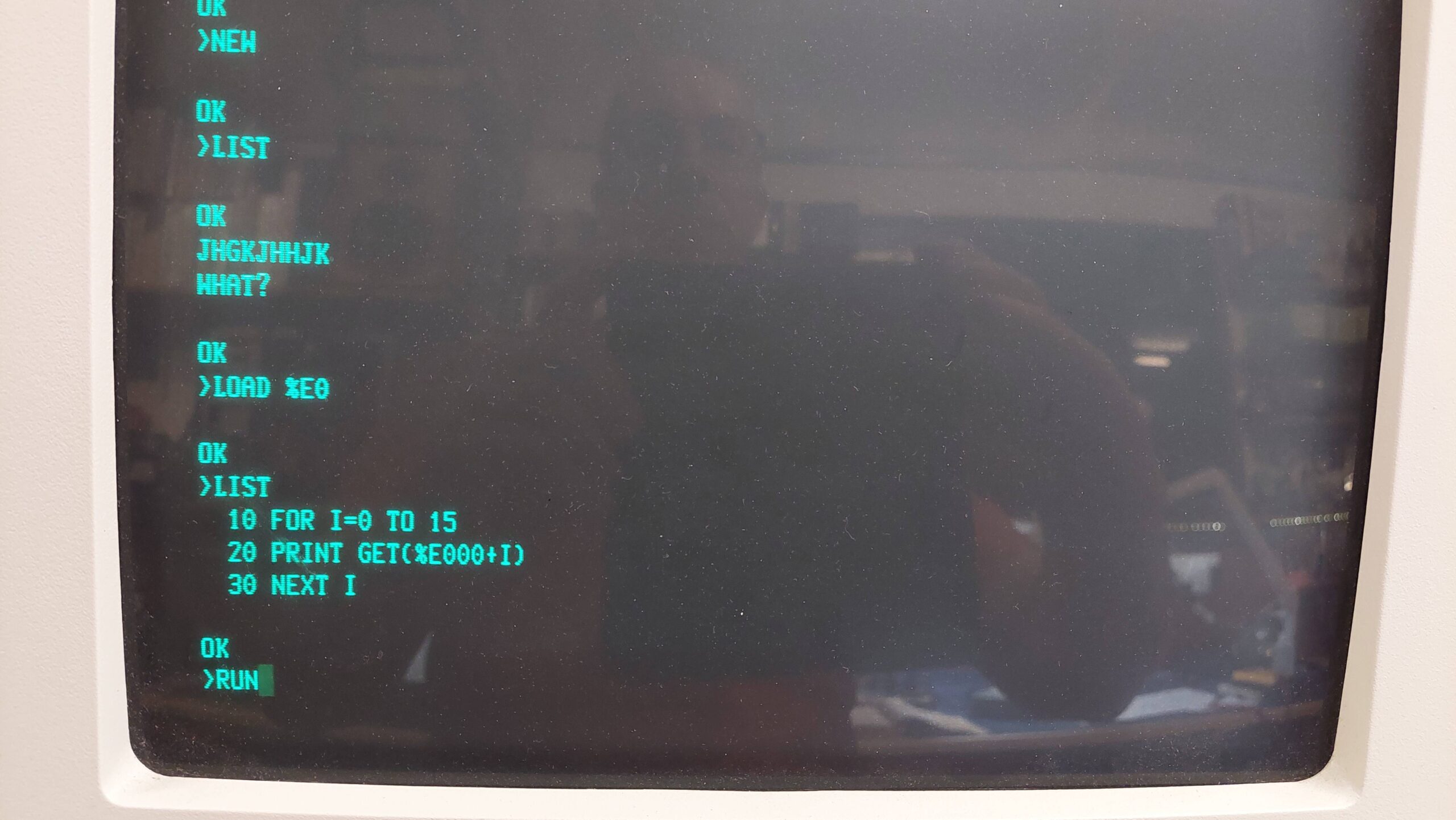
It is worth noting that it is fairly easy to accidentally overwrite an eprom. Just the random check for RAM that seems to occur when the Z80 monitor is invoked would be enough to do it. The programming switch should be set to ON only for the act of programming.
It probably doesn’t look like a big deal, but it has been a fairly painstaking effort to achieve this goal.
Apart from monitoring the reliability issue, i think the next step is to repeat the exercise with the older version of the Monitor & Basic: CB-308. This will require the binary to be programmed into two 2716 EPROMs and placed in the spare sockets of the SCC. Then the binaries can be copied into a set of 4x 2708s. This should also work on the SCC. After that, i can attempt to use the ZPU card together with some RAM and a TUART.
Other Notes:
- Top left hand blue capacitor is good for Logic Probe power. It is also good for a scope ground connection.
- A modern socket plugged into the old sockets is more accessible for buzzing out connections.
- Board_Select AND sMEMR can be picked up at IC16-1.
- MWRT can be picked up at S100-68
- CS is pin 20 on the EPROM socket
- BASIC won’t successfully quit to the Z80 monitor if the RDY signal is connected. Remove IC16-3 and connect with lead after transitioning. This needs to be resolved.
- The row of 4.7k resistors should be 18k but, this may have been due to a change for Revision 2.


